
Business Area
-
1번째 이미지 보기
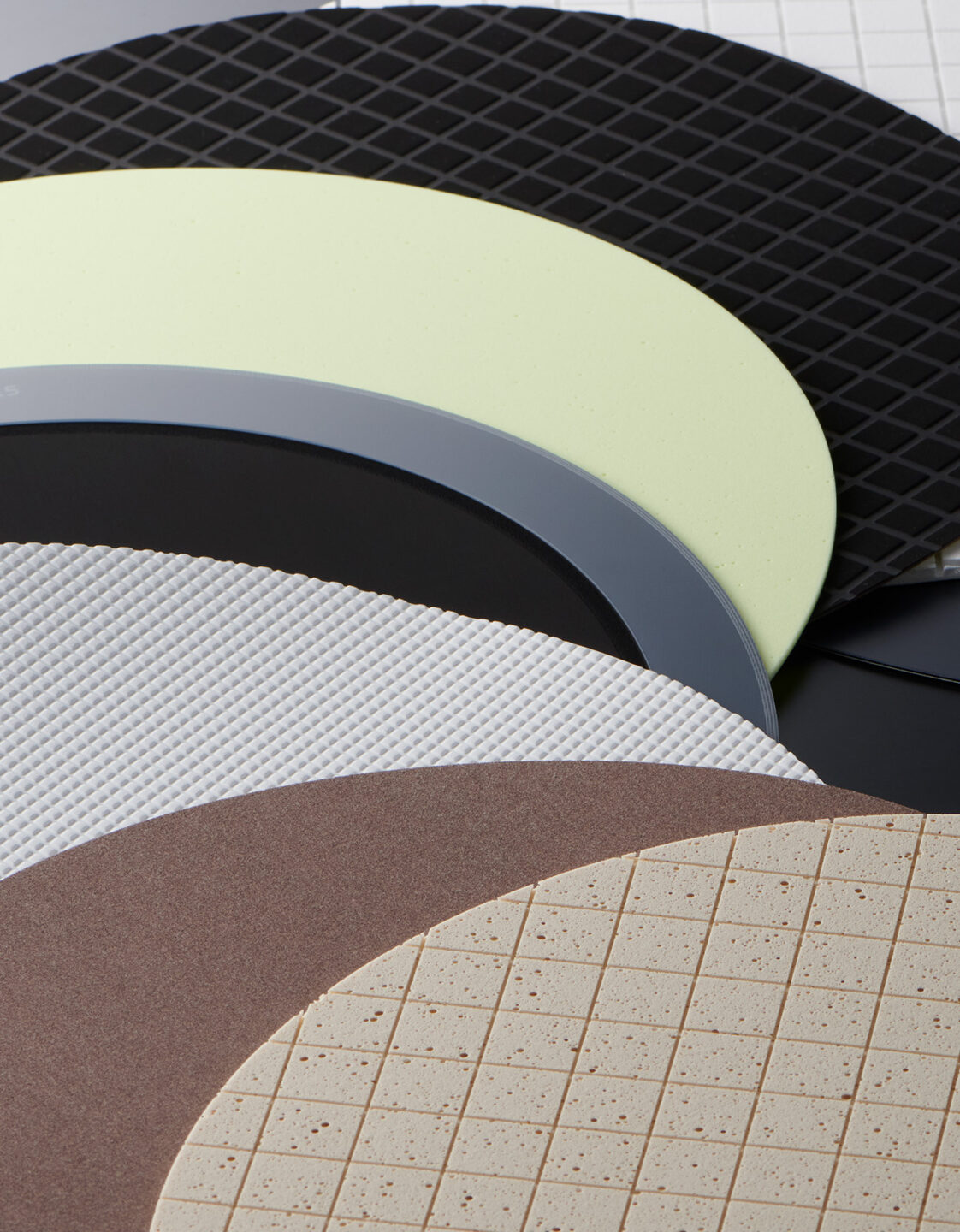
MaterialsPolishing pad, Back pad,
Manufacturer FUJIBO Ehime Co.,Ltd. Origin Japan Application • Polishing of semiconductor glass substrates and flattening of substrates related to TGV (Through Glass Via)
• Polishing of LCD glass essential for smartphones, tablets, and LCD TVs, hard disks, silicon wafers that serve as semiconductor substrates, semiconductor devices, etc.
Main Product • FP Series: Non-woven type polishing pads for primary polishing of silicon wafers, semiconductor materials, PDPs, optical lenses, metals, etc.
• FXA Series/FX Series: Non-filler/filler internally added type polishing pads developed for primary polishing of semiconductor wafers, crystal oscillators, LCD glass substrates, glass disks, optical lenses, etc.
• Suede Series: Suede type polishing pads for final polishing of semiconductor wafers, hard disks, etc.
• Back Pad Series: Back pads developed for waxless fixation of semiconductor silicon wafers and liquid crystal glass substratesMain Character • Designed for ultra-precision polishing of silicon wafers, semiconductor materials, metals, glass, etc., to obtain scratch-free, defect-free, high-precision, and high-flatness products